
perfboard-studio
Free desktop app for laying out circuits on perfboard, stripboard (veroboard) and breadboards: draw the schematic, auto-place and route it, check it with DRC and LVS, and get a step-by-step soldering guide with multimeter checkpoints. Windows, macOS, Linux.
Install / Use
claude mcp add medinstech -- npx -y github:medinstech/perfboard-studioIf the server publishes to npm under a different name, use that package instead — check the repo README.
MCP Server
Model Context Protocol server
Quality Score
Category
Development & EngineeringSupported Platforms
Our assessment of perfboard-studio
perfboard-studio scores 84/100 on our quality scale, 2767th of 4,705 Development & Engineering skills we index.
Its MCP Server is 37 KB long, well organised into 17 sections with 5 code examples: a thorough specification that gives an agent plenty to work with.
It has 10 GitHub stars, so there is little community track record yet; judge it on its content.
Maintenance, license and trust
- The repository was last updated 3 days ago, so perfboard-studio is actively maintained.
- It is released under the Apache-2.0 license, a permissive license that allows use, modification and commercial use with attribution.
- Its trust signals score 97/100, with no cautions. These come from repository metadata, not a code audit — read the skill file before letting an agent act on it.
perfboard-studio compared with similar skills
All 4 of these similar skills score higher than perfboard-studio; compare them before choosing.
| Skill | Score | Stars | Updated | Format |
|---|---|---|---|---|
| perfboard-studio (this skill)by medinstech | 84 | 10 | 3d ago | MCP Server |
| taste-skillby Leonxlnx | 100 | 120.0k | today | CLAUDE.md |
| Agent-Reachby Panniantong | 100 | 114.0k | today | CLAUDE.md |
| hyperframesby heygen-com | 100 | 88.2k | today | CLAUDE.md |
| rufloby ruvnet | 100 | 82.3k | today | CLAUDE.md |
Frequently asked questions
- How do I install perfboard-studio?
- Run
claude mcp add medinstech -- npx -y github:medinstech/perfboard-studio. The install tabs above show the steps for each supported agent. - Which AI agents does perfboard-studio work with?
- It is written for Claude Code and Claude Desktop, as a MCP Server file. Other agents that read the same format can often use it too.
- Is perfboard-studio safe to use?
- It is Apache-2.0-licensed and scores 97/100 on trust signals. Skills are instructions an agent will follow, so read the file before installing it and do not approve commands you do not understand.
- Is perfboard-studio still maintained?
- The repository was last updated 3 days ago, so perfboard-studio is actively maintained.
Skill content
View source on GitHub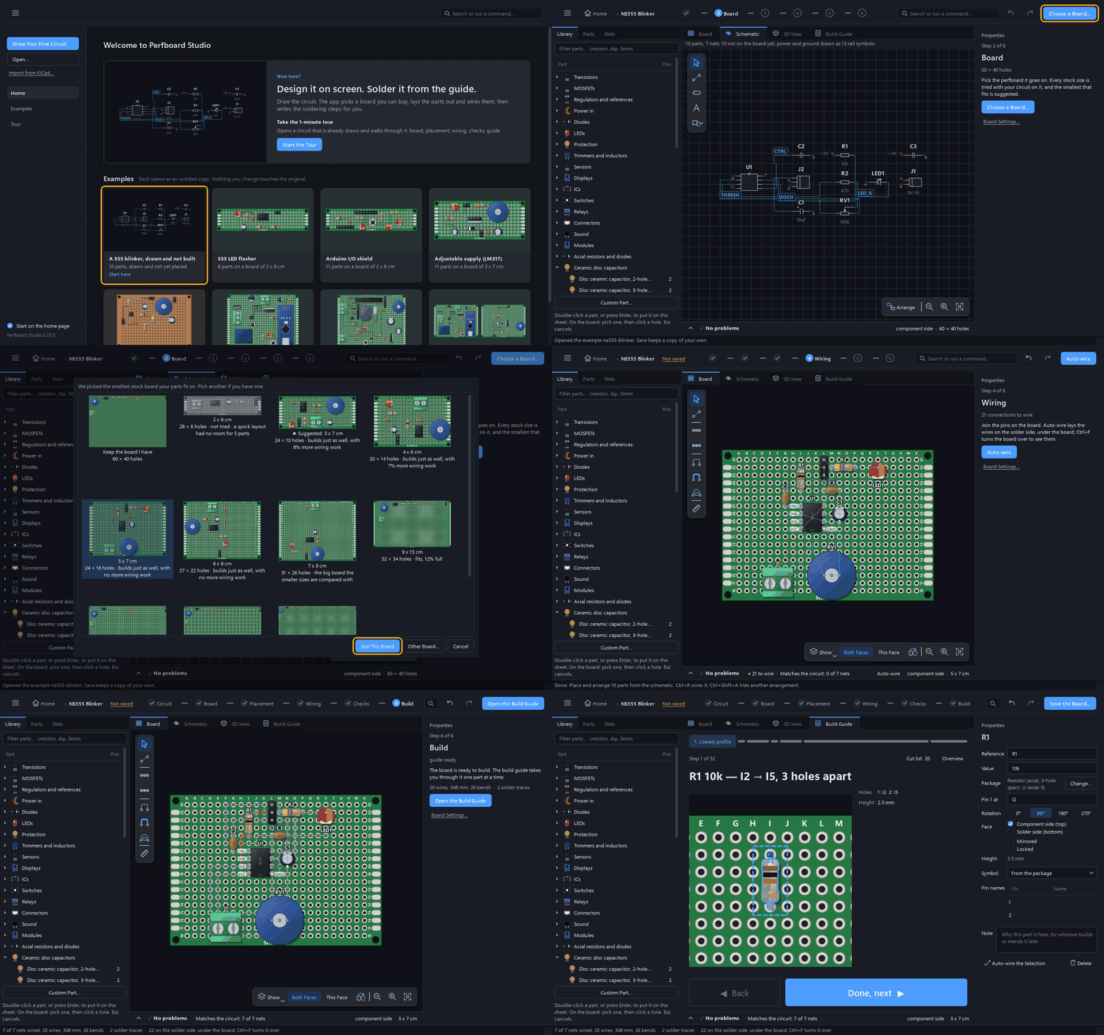
New here? Your first board, from Home to the build guide takes the 555 blinker through every step above in about ten minutes.
Perfboard Studio is made for boards that are soldered by hand, and three things follow from that. A solder trace and a wire are different connections with different costs and limits, and the router chooses between them. The build guide is a sequence of steps with checkpoints to measure, in the order you solder in. And the board is checked against the circuit by extracting what is really connected, which for perfboard means the copper you laid.
- A soldering guide with verification steps. Not just "solder R1 here", but "block 2 complete → U1 pin 4 to C3(−) must show continuity" and "before power-on: GND to V+ must read above 10 kΩ". Derived from the netlist, so it is exact rather than generic advice.
- The circuit is checked, then the board. While the circuit is still being drawn, ERC catches a chip whose supply pin is wired to nothing, an electrolytic or an LED drawn the wrong way round, a net that reaches only one pin, and a supply that no connector or battery brings onto the board. Once it is on the board, perfboard LVS extracts the board's real connectivity and compares it against the schematic: opens, shorts and floating conductors are reported before you pick up the iron.
- Six kinds of connection, not one. A lead bend, a solder trace, a wired solder trace, bare wire, insulated wire and a jumper over the parts have different costs, limits and failure modes, and the router prices all six — which is what makes a layout that is pleasant to actually solder.
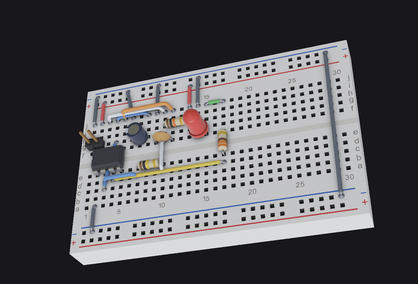
- A breadboard first, then the perfboard. A solderless breadboard is a board type too: placed, wired with jumpers and power down the rails, and given a building guide with no iron in it. When the circuit works, the same design goes on to perfboard — or onto a solderable breadboard, hole for hole.
- Four rules only the third dimension can see. A part too tall for the case, a jumper trapped under a body that gets soldered down on top of it, a heat-sensitive part sitting too close to a hot one, and a part tucked under a module's raised board, where nobody can reach it once the module is on. The 3D view is a checking tool, not a picture — and the board leaves as a STEP model of the same bodies, to draw its case round.
- Real parts, by name. Pick a BC547, a 7805 or an Arduino Nano out of the catalog and it arrives with what its datasheet calls every lead. A KiCad netlist, if you have one, comes in the same way — and where its symbol numbers the pins differently from the part in your hand, they are renumbered by name, so the board is wired for the part you actually solder.
- Agent-native. An MCP server, a headless CLI and a git-diffable project file, all driving the same command bus as the GUI — so undo works across a session where a human and a model both edit the board.
Status: pre-alpha, and end to end. A circuit goes in and a soldering guide comes out. What is missing is the dogfood test — nobody has yet built a real board by following a generated guide, and the project plan says M5 does not close until somebody has. Everything else runs, and every release ships an installer for each of the three desktop platforms, none code-signed.
Jump to — Running it · Connections · Both faces · Real parts · The schematic · The guide · From an agent · How it is built · Documentation · Contributing
Connections are not all the same thing
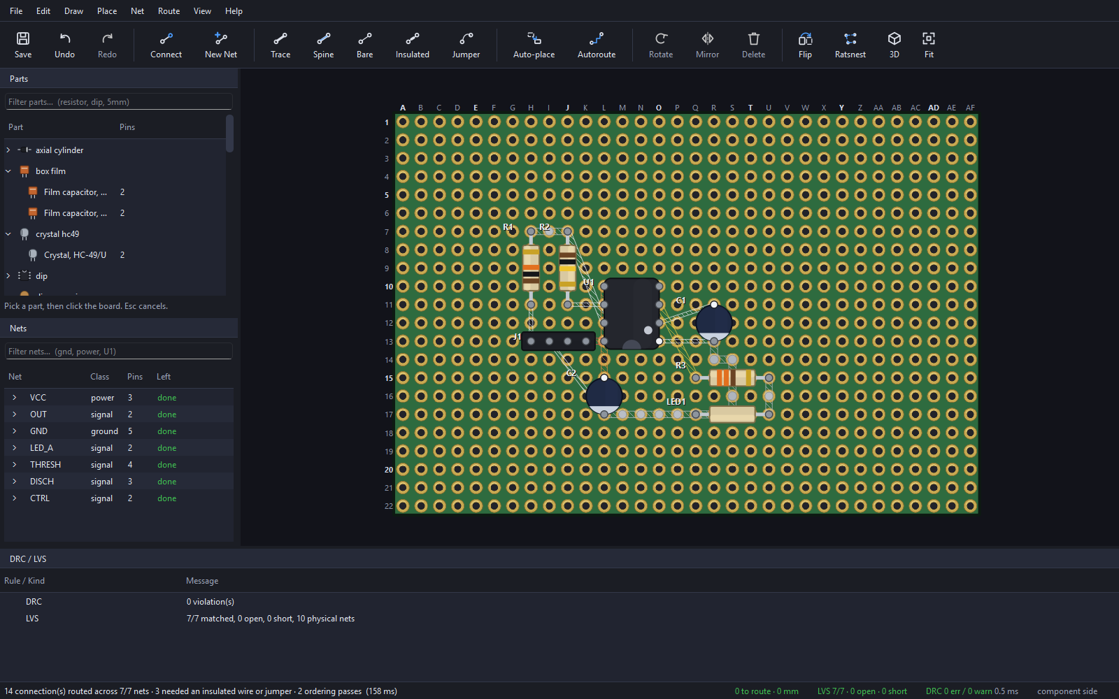
Most tools model a perfboard connection as "a wire". Perfboard has six physically distinct ways to join two points, each with its own cost, limits and failure modes — and modelling that difference is what lets the router produce a layout that is pleasant to actually solder:
| | what it is | notes | |---|---|---| | lead bend | a component leg bent to a nearby hole | effectively free, 3–4 holes | | solder trace | adjacent pads joined with solder alone | orthogonal only; ~0.6 mm to the next pad | | reinforced solder trace | the same, laid over a tinned wire | ~10× lower resistance, no length limit | | bare wire | tinned wire on the solder side | cannot cross another bare conductor | | insulated wire | may cross freely | costs preparation time | | jumper over the parts | insulated jumper on the component side | visible, occupies body space |
The 0.6 mm gap to the neighbouring pad is why solder traces are both so useful and so easy to get wrong. Perfboard Studio scores that risk into the router's cost function, and turns every flagged spot into a measurement step in the build guide.
Or no solder at all. A solderless breadboard is a board type too, in the three sizes it
is sold in, and its holes are named the way it prints them — e12, row letter first. The
placer keeps two nets out of one clip and puts each chip across the groove, the router runs
jumpers into free holes and ground and power down the rails, and the guide becomes a
building guide: jumpers first, flat on the plastic, and no iron anywhere. When the circuit
works, File ▸ New Board from This Design… takes it on to perfboard, and the breadboard's
file stays as it was. Or File ▸ Same Layout on a Solderable Breadboard… puts it on a
solderable one — the same holes and strips in copper — with every part and jumper on the
holes it had, and the guide that comes with it is a soldering guide again.
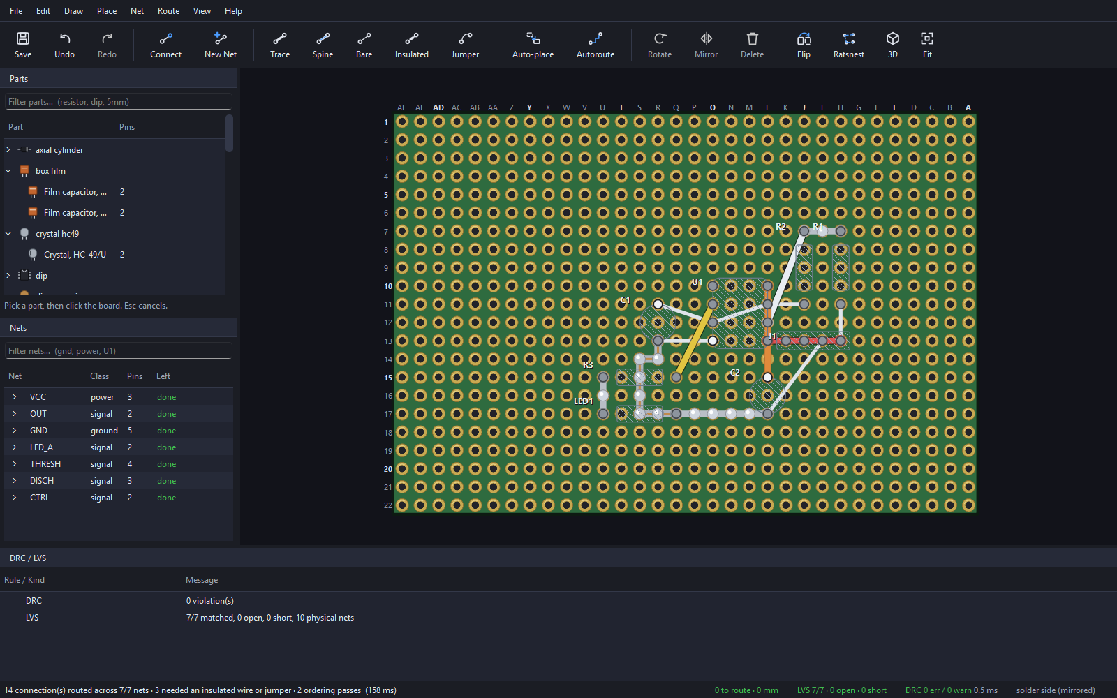
Both faces, and the third dimension
The solder side is where the copper is, so it is a first-class view rather than a mirror mode — and copper on the face you are not looking at is hatched, because a board is opaque and a trace drawn solid says this is in front of you.
And copper goes on either face. On a board with pads on both faces, what you draw goes on the face you are looking at, and a net can be given a face of its own — Either, Component Side or Solder Side in its Properties — which Auto-wire keeps it on wherever it can. A trace changes face through a pin of its own net, or through an empty hole the guide has you fill and then probe; a pin that a seated part covers on that face is reached by a wire that ends in the free hole beside it, and a short lead offcut underneath joins that hole to the pin. Where a net could not stay on its face, Auto-wire says which connections left it and why.
The 3D view is a checking tool, not a picture. Four rules exist that a top-down view cannot see at all: a part too tall for the case, a jumper trapped under a body that will be soldered down on top of it, a heat-sensitive part sitting too close to a hot one, and a part under a module's raised board — which from above looks like an overlap, and which fits, but cannot be reached once the module is on.
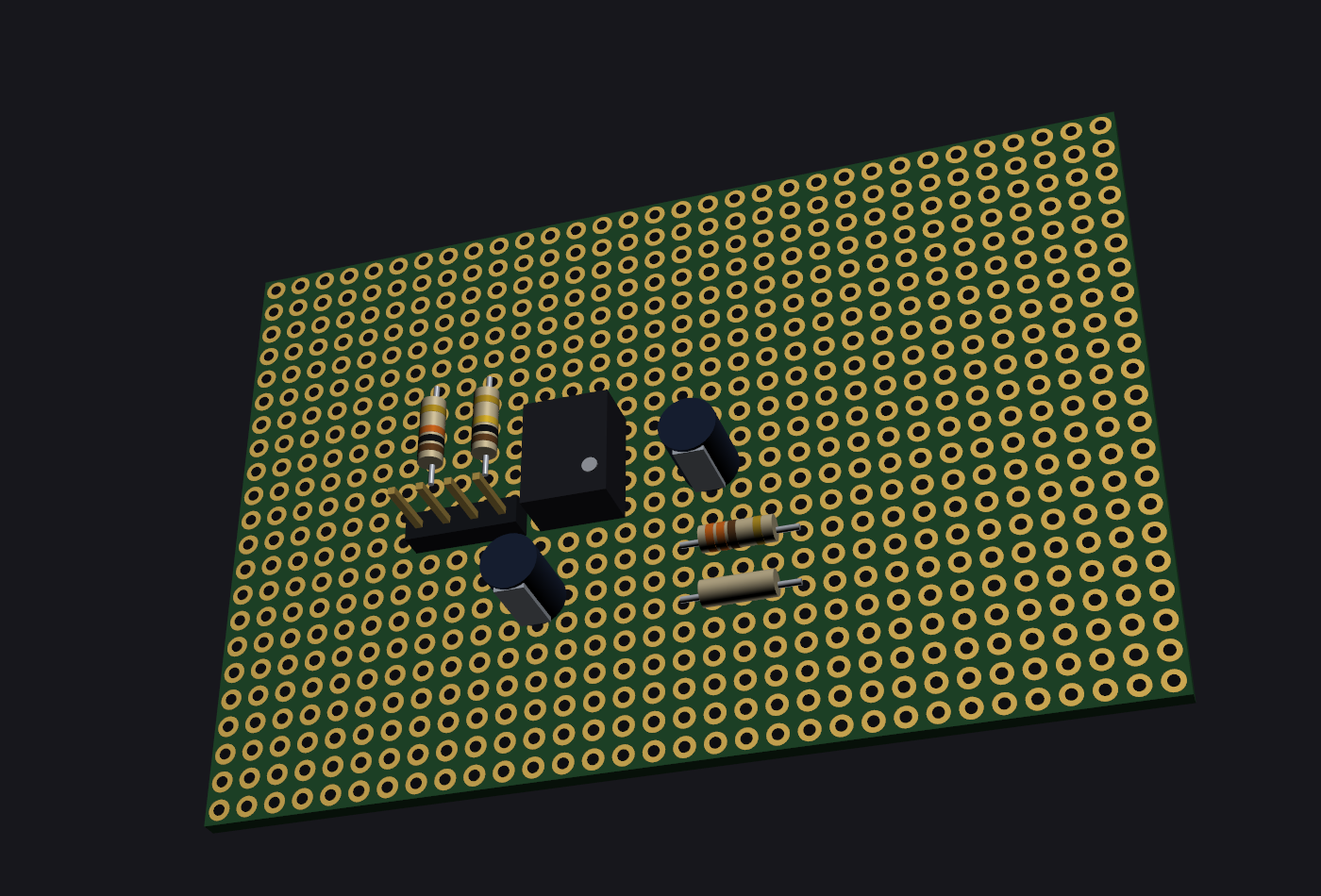
It stands beside the board, and it answers a click. Board, schematic, 3D and the build guide are tabs over one canvas, and a tab dragged aside stands beside the others. A part clicked in 3D is selected on the board and on the sheet, and the build guide goes to its step; a wire clicked there lights its net everywhere; and whatever is selected anywhere is tinted in 3D, so the three views show one selection.
And it leaves as STEP. File ▸ Export ▸ 3D Model (STEP)… writes the board as solids a mechanical CAD program can measure and cut a box round: the board with every hole and mounting bore through it, each part as the room it takes — the very outline and height DRC's overhang and too-tall rules measure — every lead down through its hole, and every wire as thick as the gauge the cut list prints, lifted over whatever it crosses. The application writes the file itself, so it needs no graphics driver and no extra dependency, and a project save puts on
Truncated for display — read the full file on GitHub.
Related Skills
taste-skill
120.0kAgent skills that give coding agents taste: art direction, reference images and a browser check instead of generic AI pages
Agent-Reach
114.0kGive your AI agent eyes to see the entire internet. Read & search Twitter, Reddit, YouTube, GitHub, Bilibili, XiaoHongShu — one CLI, zero API fees.
hyperframes
88.2kAI video you can actually edit. HyperFrames is a free, open-source AI video editor. Describe any video and get a real project you can change down to the frame.
ruflo
82.3k🌊 The original agent harness. Deploy intelligent multi-player swarms, coordinate autonomous workflows, and build conversational AI systems. Features adaptive memory, self-learning intelligence, federation, vector RAG integration, and native Claude Code / Codex / Hermes and many more Integrated

Languages
Trust signals
From repository metadata: license, adoption, age and documentation. Not a code audit — see the Safety scan above for what the skill file itself contains.